
Benign Design for the Environment
Air Date: Week of October 9, 2009
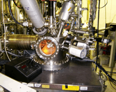
Photo courtesy of National Science Foundation.
Semiconductor manufacturing plants need lots of water to operate. As the industry grows, it’s scrambling to find ways to save water and cut costs. As part of IEEE Spectrum Magazine and the National Science Foundation's "The Global Water Challenge" series, producer Laurie Howell visits an engineering research center in Arizona where engineers are devising new technologies for saving water and for other environmental challenges.
Transcript
YOUNG: Semiconductors are the building blocks of modern electronics – making our products smarter. But the way semiconductors are made isn’t always so smart when it comes to water. A single manufacturing plant can use as much water as a small city. One place in Arizona is working to turn those water guzzlers into sippers. It’s the Engineering Research Center for Environmentally Benign Semiconductor Manufacturing. Yeah, it’s a long name. But as Laurie Howell reports for the IEEE Spectrum Magazine and the National Science Foundation's "The Global Water Challenge" series, the engineers and students there also have a long list of water saving ideas.
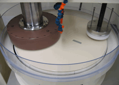
Polisher (Photo courtesy of National Science Foundation).
[SOUND OF POLISHER]
HOWELL: This mini-computer chip manufacturing plant is a test facility. Located in a warehouse on the University of Arizona campus, it’s where engineers recreate the industry’s water problems so they can fix them.
SUN: So, here is a typical 200-millimeter polisher – looks like – at the bottom is the rotating pad…
HOWELL: Chemical Engineer Ting Sun gives me a tour of the polishing room, lined with various sizes of flat, round silicon wafers.
SUN: And when we’re ready, we’re gonna bring the head down and the wafer will touch the pad. All of them are rotating, so they’re gonna do the polish work.
HOWELL: Polishers spin the silicon wafers against a pad and a chemical mix known as slurry, polishing each layer of circuitry and then rinsing it with ultra pure water. Sun has focused her research on engineering better pads.
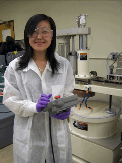
Chemical engineer Ting Sun. (Photo courtesy of National Science Foundation.)
TING SUN: By doing that, we can use less chemicals, so we dump less chemical into the environment, so that helps a lot, and also by using less of chemical, we also use less water to rinse it.
HOWELL: Sun is schooled in a practice called “design for the environment,” a strategy that guides the center’s operations. Farhang Shadman directs the engineering research center.
SHADMAN: “Design for environment” basically means that those who are in charge of developing new processes will have the environmental, not only environmental thinking but also the tools and techniques of environmental assessment in their way of doing research.
HOWELL: The center’s full name is SRC/Sematech Engineering Research Center for Environmentally Benign Semiconductor Manufacturing. Under Shadman’s leadership, it’s grown to include nine US universities, since its 1996 launch.

/Farhang Shadman (left) and doctoral student Kedar Dhane. (Courtesy of National Science Foundation.)
SHADMAN: Probably the legacy of the center is showing and proving, by many, many examples, that environmental approach to technology not only makes sense, not only it reduces cost, it may be the only way that future manufacturing is done.
HOWELL: Computer chip makers watch this center closely for new technologies, and it’s easy to understand why. Many semiconductor manufacturing plants are located in the water strapped cities of the Southwest.
SHADMAN: One manufacturing plant uses anywhere between two to four million gallons of very, very pure water, we call it ultra-pure water, per day, and that, on the average, is roughly equivalent to the water usage of a city of maybe 40 or 50,000 people.
Semiconductor (Courtesy of National Science Foundation)
HOWELL: Shadman guides me past a room with engineers dressed head to toe in what they call “cleanroom suits,” which protect the research from outside impurities. Just like surgery, semiconductor manufacturing requires a sterile environment.
SHADMAN: OK, what you see here is what we call a pilot plant, a water pilot plant, and it is very unique because it essentially resembles the water purification plants of semiconductor manufacturing except that everything is in smaller scale and everything is research development oriented so we can change things, things that you can not do in the real manufacturing.
HOWELL: So, what we’re looking at right here are different stations where the water goes through purification process, water softeners, carbon filters. And that’s because the water that’s needed in the semiconducting industry needs to be so pure, purer than any water, anywhere.
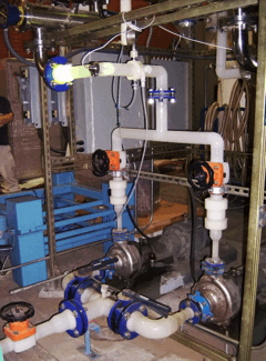
Water Purifier (Courtesy of National Science Foundation.)
SHADMAN: Yes, because the wafer that is being cleaned is already very clean. You’re trying to remove very, very small traces of impurity. So, if water has any contaminants in it, it will be harmful. Very interesting point is about bacteria. We cannot tolerate any bacteria – live or dead – it doesn’t matter, because of the fact that the bacteria typically have some of the trace elements in them like phosphorus, like carbon. These traces of these compounds would change the electrical properties of the silicon wafer.
HOWELL: And that could lead to defective computer chips and, ultimately, product recalls. So, chemical engineer Jun Yan has been developing a new water sensor that immediately detects when a silicon wafer is clean, so rinsing can stop, saving millions of gallons of water a day.
YAN: Environmental concern, environmental issue and how mankind, the civilization can survive depend on what can we do and how can we approach it, so I think it’s very exciting, you know, it’s very important, meaningful work.

Chemical engineer Jun Yan. (Photo courtesy of National Science Foundation.)
HOWELL: The water sensor developed by Yan and his colleagues is already on the market and was named 2009 product of the year by SEMI, a global association for microelectronics and other industries. Again, Farhang Shadman.
SHADMAN: We want to make sure that manufacturing, particularly high technology manufacturing, is maintained and retained, kept in the United States, and if you do not solve some of these environmental issues and some of these resource issues, we stand the risk of losing that manufacturing to other areas.
HOWELL: The Center has now spun off five start-up companies. And, its environmental technologies are being applied outside semiconductor manufacturing and electronics, including the medical and pharmaceutical industries. For Living on Earth, I'm Laurie Howell in Tucson, Arizona.
YOUNG: Laurie Howell reported this story for the Global Water Challenge, a co-production of IEEE Spectrum magazine and the Directorate of Engineering for the National Science Foundation.
Links
SRC/Sematech Engineering Research Center for Environmentally Benign Semiconductor Manufacturing.
Living on Earth wants to hear from you!
Living on Earth
62 Calef Highway, Suite 212
Lee, NH 03861
Telephone: 617-287-4121
E-mail: comments@loe.org
Newsletter [Click here]
Donate to Living on Earth!
Living on Earth is an independent media program and relies entirely on contributions from listeners and institutions supporting public service. Please donate now to preserve an independent environmental voice.
NewsletterLiving on Earth offers a weekly delivery of the show's rundown to your mailbox. Sign up for our newsletter today!
![]() Sailors For The Sea: Be the change you want to sea.
Sailors For The Sea: Be the change you want to sea.
 The Grantham Foundation for the Protection of the Environment: Committed to protecting and improving the health of the global environment.
 Contribute to Living on Earth and receive, as our gift to you, an archival print of one of Mark Seth Lender's extraordinary wildlife photographs. Follow the link to see Mark's current collection of photographs.
 Buy a signed copy of Mark Seth Lender's book Smeagull the Seagull & support Living on Earth
© Copyright World Media Foundation. All Rights Reserved
Home | Contact | RSS | Donate | Newsletter